Electrical Engineering > QUESTIONS & ANSWERS > University of California, Los Angeles - EC ENGR 115CHw-05-W12-Sol (All)
University of California, Los Angeles - EC ENGR 115CHw-05-W12-Sol
Document Content and Description Below
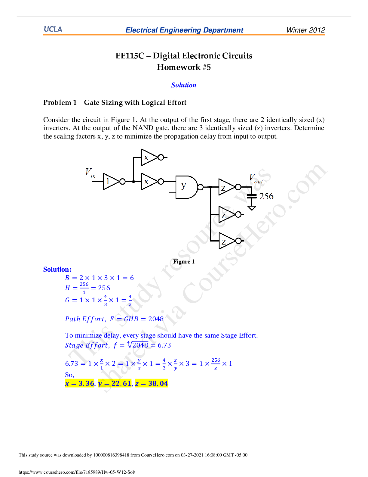
EE115C – Digital Electronic Circuits Homework #5 Solution Problem 1 – Gate Sizing with Logical Effort Consider the circuit in Figure 1. At the output of the first stage, there are 2 identicall... y sized (x) inverters. At the output of the NAND gate, there are 3 identically sized (z) inverters. Determine the scaling factors x, y, z to minimize the propagation delay from input to output. Figure 1 Solution: To minimize delay, every stage should have the same Stage Effort. √ So, , , [Show More]
Last updated: 2 years ago
Preview 1 out of 3 pages
Buy this document to get the full access instantly
Instant Download Access after purchase
Buy NowInstant download
We Accept:

Reviews( 0 )
$7.00
Can't find what you want? Try our AI powered Search
Document information
Connected school, study & course
About the document
Uploaded On
Mar 28, 2021
Number of pages
3
Written in

Additional information
This document has been written for:
Uploaded
Mar 28, 2021
Downloads
0
Views
63


.png)