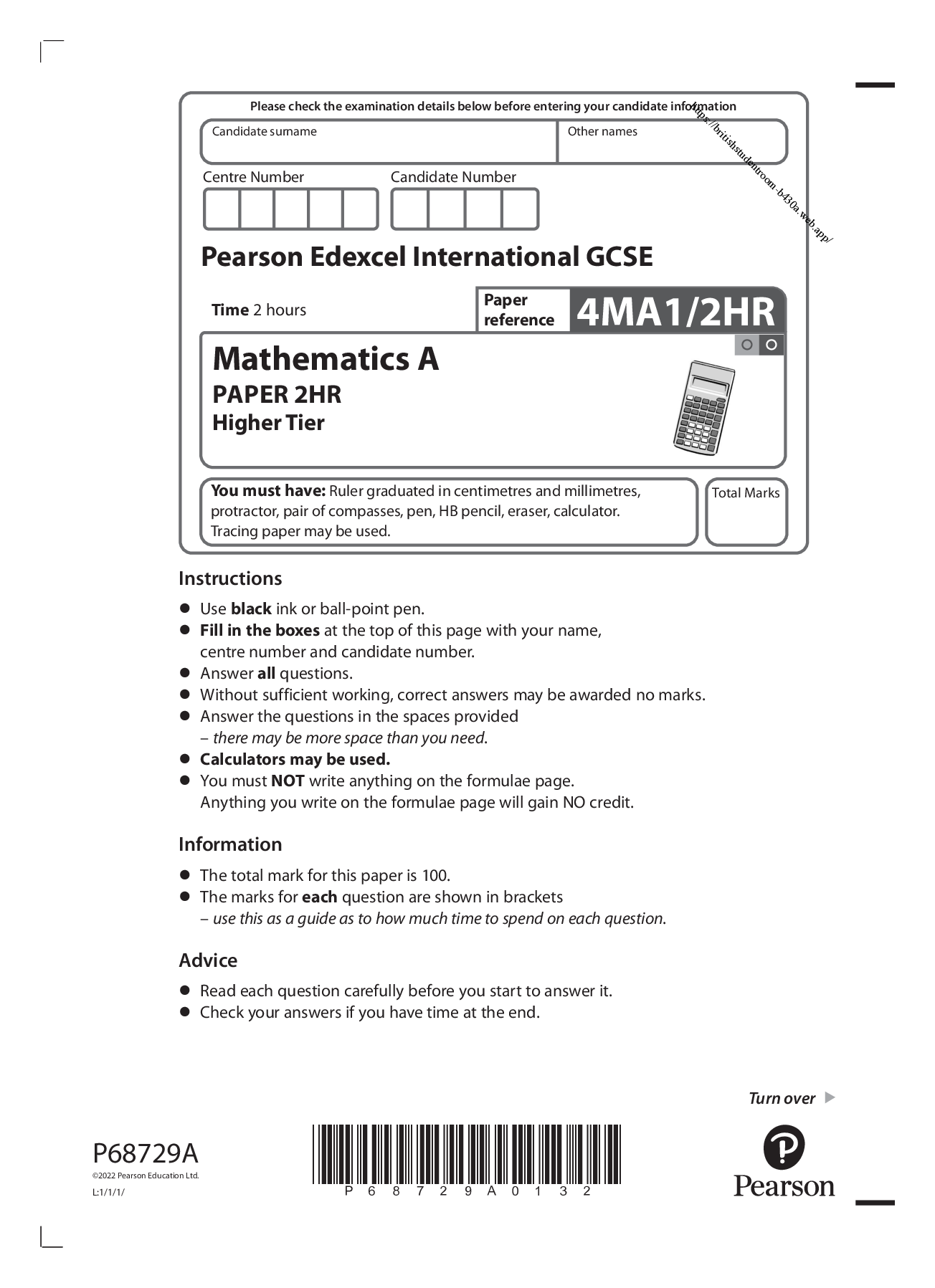
Pearson Edexcel International GCSE_Mathematics A_4MA1/2HR Question Paper Jan 2022 | PAPER 2HR
Physics > QUESTION PAPER & MARK SCHEME > AQA A-level PHYSICS 7408/3BE Paper 3 Section B Electronics Question Paper + Mark scheme (Merged) GRA (All)
A-level PHYSICS 7408/3BE Paper 3 Section B Electronics Question Paper + Mark scheme (Merged) June 2021 Version: 1.0 Final *JUN2174083BE01* IB/M/Jun21/E8 7408/3BE For Examiner’s Use Question ... Mark 1 2 3 4 5 TOTAL Materials For this paper you must have: • a pencil and a ruler • a scientific calculator • a Data and Formulae Booklet • a protractor. Instructions • Use black ink or black ball-point pen. • Fill in the boxes at the top of this page. • Answer all questions. • You must answer the questions in the spaces provided. Do not write outside the box around each page or on blank pages. • If you need extra space for your answer(s), use the lined pages at the end of this book. Write the question number against your answer(s). • Do all rough work in this book. Cross through any work you do not want to be marked. • Show all your working. Information • The marks for questions are shown in brackets. • The maximum mark for this paper is 35. • You are expected to use a scientific calculator where appropriate. • A Data and Formulae Booklet is provided as a loose insert. Please write clearly in block capitals. Centre number Candidate number Surname Forename(s) Candidate signature I declare this is my own work. A-level PHYSICS Paper 3 Section B Electronics Time allowed: The total time for both sections of this paper is 2 hours. You are advised to spend approximately 50 minutes on this section. 2 *02* IB/M/Jun21/7408/3BE Do not write outside the box Section B Answer all questions in this section. 0 1 Figure 1 shows a simplified structure of an N-channel enhancement mode MOSFET. Figure 1 0 1 . 1 State the name of the part shown in this MOSFET structure that causes the input resistance to be very large. [1 mark] 0 1 . 2 Which terminal of the MOSFET is connected directly to 0 V when it is used as a simple switch? Tick () one box. [1 mark] drain gate source 3 *03* Turn over ► IB/M/Jun21/7408/3BE Do not write outside the box Figure 2 shows how the drain–source current IDS of the MOSFET varies with drain–source voltage VDS for a range of gate–source voltages VGS. Figure 2 The MOSFET is used as a simple switch in a filament lamp circuit. The circuit uses power rails of 12 V and 0 V. The resistance of the lamp is 154 Ω when operating at its full power of 0.65 W. 0 1 . 3 Deduce the minimum value of VGS needed for the lamp to operate at full power. [2 marks] VGS = V [Show More]
Last updated: 3 years ago
Preview 1 out of 40 pages
.png)
Buy this document to get the full access instantly
Instant Download Access after purchase
Buy NowInstant download
We Accept:

Can't find what you want? Try our AI powered Search
Connected school, study & course
About the document
Uploaded On
Dec 11, 2022
Number of pages
40
Written in
All
This document has been written for:
Uploaded
Dec 11, 2022
Downloads
0
Views
113
Scholarfriends.com Online Platform by Browsegrades Inc. 651N South Broad St, Middletown DE. United States.
We're available through e-mail, Twitter, Facebook, and live chat.
FAQ
Questions? Leave a message!
Copyright © Scholarfriends · High quality services·