Computer Science > Lab Experiment > University of Texas, Dallas - CS 4141experiment-4. Familiarization with Sequential Logic Circuits ( (All)
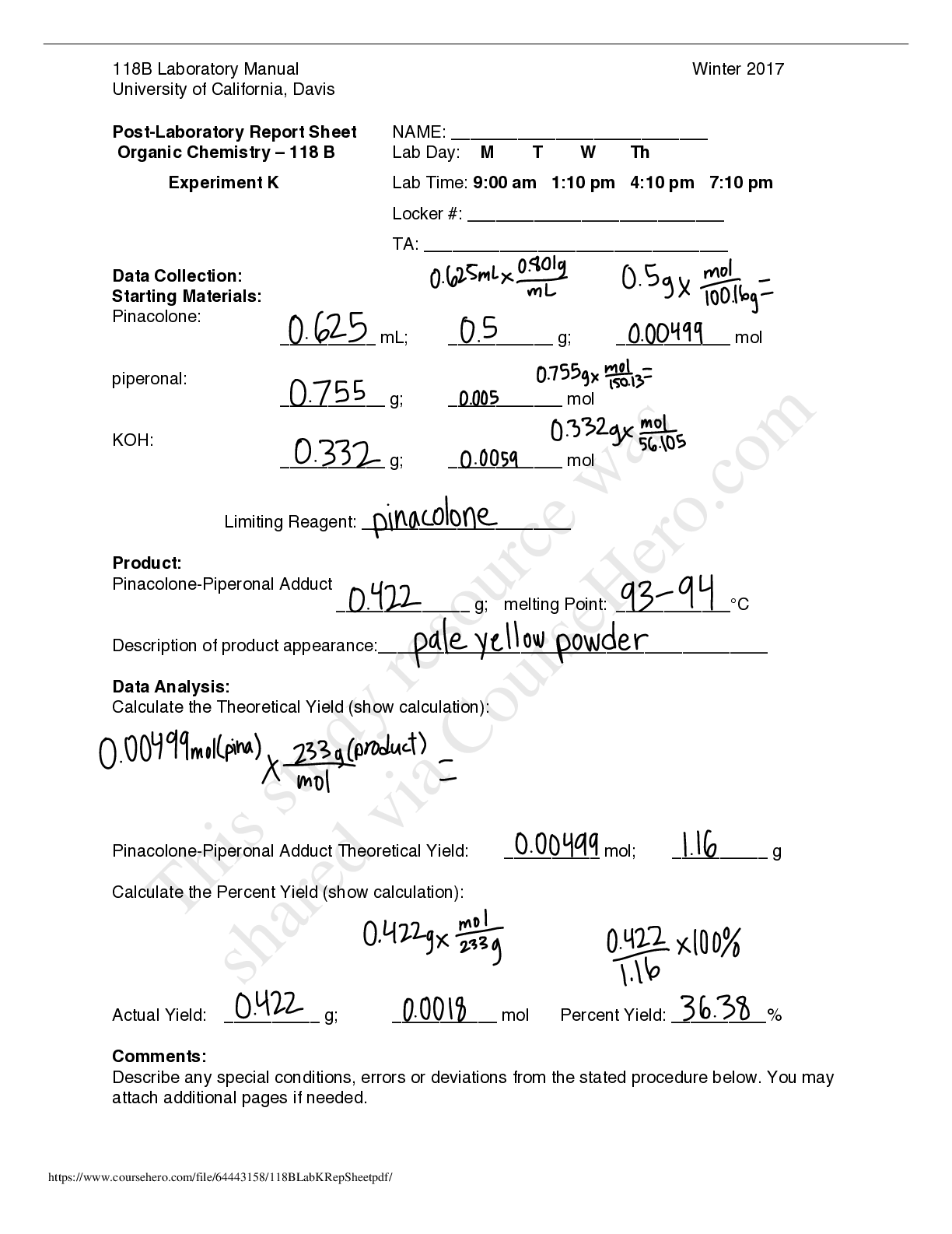
University of Texas, Dallas - CS 4141experiment-4. Familiarization with Sequential Logic Circuits (Flip-Flops)
Document Content and Description Below
Last updated: 7 months ago
Preview 1 out of 3 pages
Instant download

Buy this Document to get the Full Access Instantly
Provided by Students Who Aced it
We Verify Document Content to Gurantee Accuracy
Reviews( 0 )
Document information
Connected school, study & course
About the document
Uploaded On
Apr 06, 2021
Number of pages
3
Written in
All

Additional information
This document has been written for:
Uploaded
Apr 06, 2021
Downloads
0
Views
260
Topic Tags
Recommended For You
Get more on Lab Experiment »
Solutions Manual For Building Java Programs A Back to Basics A...
Test Bank For Building Java Programs A Back to Basics Approach...
Solutions Manual For Building Java Programs A Back to Basics A...
Solutions Manual For Art and Science of Leadership, The, 8th E...

Solutions Manual for Real Analysis: Foundations by Sergei Ovch...
Computer Systems Application 1st Edition By Viktor Boradin eBo...

eBook [PDF] An Introduction to Optimization With Applications...

Test Bank For Art and Science of Leadership, The, 8th Edition...

eBook Advanced Two-Dimensional Material-Based Heterostructures...
Introduction to Cryptography with Coding Theory, 3rd edition b...

Introduction to Python for Computer Science and Data Science,...
TEST BANK for Intro to Python for Computer Science and Data Sc...
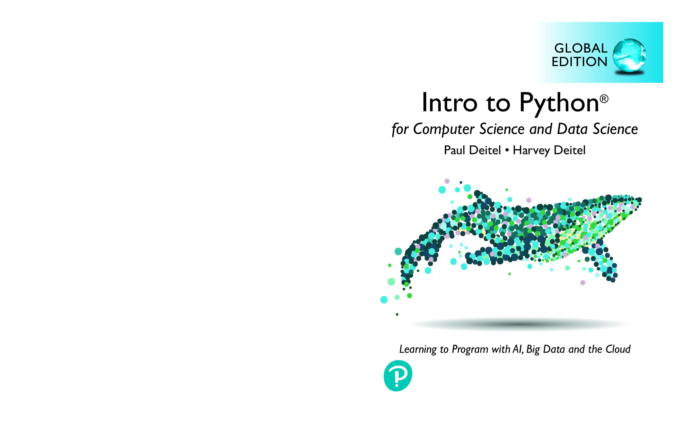
eBook Intro to Python for Computer Science and Data Science Le...
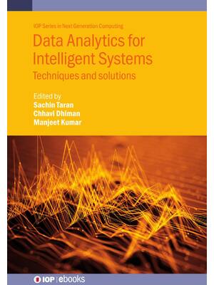
PDF(eBook) Data Analytics for Intelligent Systems 1st Edition...



.png)


