1.3 / KEY TERMS AND REVIEW QUESTIONS 15
Key Terms
Review Questions
1.1. What, in general terms, is the distinction between computer organization and computer architecture?
1.2. What, in general terms, is the distinct
...
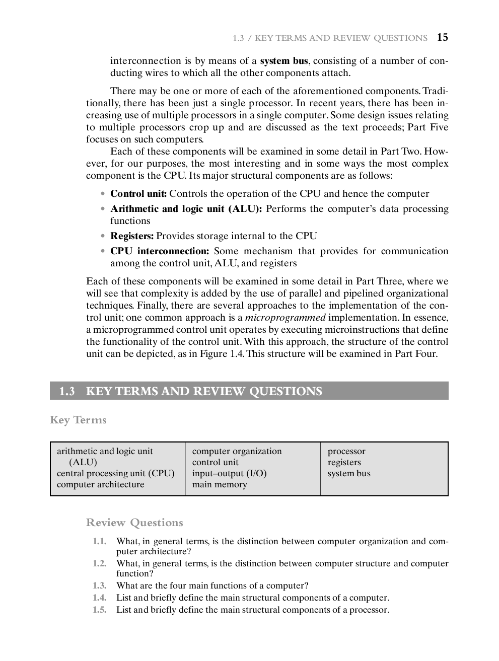
1.3 / KEY TERMS AND REVIEW QUESTIONS 15
Key Terms
Review Questions
1.1. What, in general terms, is the distinction between computer organization and computer architecture?
1.2. What, in general terms, is the distinction between computer structure and computer
function?
1.3. What are the four main functions of a computer?
1.4. List and briefly define the main structural components of a computer.
1.5. List and briefly define the main structural components of a processor.
interconnection is by means of a system bus, consisting of a number of conducting wires to which all the other components attach.
There may be one or more of each of the aforementioned components. Traditionally, there has been just a single processor. In recent years, there has been increasing use of multiple processors in a single computer. Some design issues relating
to multiple processors crop up and are discussed as the text proceeds; Part Five
focuses on such computers.
Each of these components will be examined in some detail in Part Two. However, for our purposes, the most interesting and in some ways the most complex
component is the CPU. Its major structural components are as follows:
• Control unit: Controls the operation of the CPU and hence the computer
• Arithmetic and logic unit (ALU): Performs the computer’s data processing
functions
• Registers: Provides storage internal to the CPU
• CPU interconnection: Some mechanism that provides for communication
among the control unit, ALU, and registers
Each of these components will be examined in some detail in Part Three, where we
will see that complexity is added by the use of parallel and pipelined organizational
techniques. Finally, there are several approaches to the implementation of the control unit; one common approach is a microprogrammed implementation. In essence,
a microprogrammed control unit operates by executing microinstructions that define
the functionality of the control unit. With this approach, the structure of the control
unit can be depicted, as in Figure 1.4. This structure will be examined in Part Four.
1.3 KEY TERMS AND REVIEW QUESTIONS
arithmetic and logic unit
(ALU)
central processing unit (CPU)
computer architecture
computer organization
control unit
input–output (I/O)
main memory
processor
registers
system bus
2.7 / KEY TERMS, REVIEW QUESTIONS,AND PROBLEMS 59
• Standard Performance Evaluation Corporation: SPEC is a widely recognized organization in the computer industry for its development of standardized benchmarks
used to measure and compare performance of different computer systems.
• Top500 Supercomputer Site: Provides brief description of architecture and organization of current supercomputer products, plus comparisons.
• Charles Babbage Institute: Provides links to a number of Web sites dealing with the
history of computers.
2.7 KEY TERMS, REVIEW QUESTIONS,AND PROBLEMS
Key Terms
accumulator (AC)
Amdahl’s law
arithmetic and logic unit (ALU)
benchmark
chip
data channel
embedded system
execute cycle
fetch cycle
input-output (I/O)
instruction buffer register (IBR)
instruction cycle
instruction register (IR)
instruction set
integrated circuit (IC)
main memory
memory address register
(MAR)
memory buffer register (MBR)
microprocessor
multicore
multiplexor
opcode
original equipment manufacturer (OEM)
program control unit
program counter (PC)
SPEC
stored program computer
upward compatible
von Neumann machine
wafer
word
Review Questions
2.1. What is a stored program computer?
2.2. What are the four main components of any general-purpose computer?
2.3. At the integrated circuit level, what are the three principal constituents of a computer
system?
2.4. Explain Moore’s law.
2.5. List and explain the key characteristics of a computer family.
2.6. What is the key distinguishing feature of a microprocessor?
Problems
2.1. Let A A(1), A(2), ..., A(1000) and B B(1), B(2), ..., B(1000) be two vectors
(one-dimensional arrays) comprising 1000 numbers each that are to be added to form
an array C such that C(I) A(I) B(I) for I 1, 2, ..., 1000. Using the IAS instruction set, write a program for this problem. Ignore the fact that the IAS was designed to have only 1000 words of storage.
2.2. a. On the IAS, what would the machine code instruction look like to load the contents of memory address 2?
b. How many trips to memory does the CPU need to make to complete this instruction during the instruction cycle?
2.3. On the IAS, describe in English the process that the CPU must undertake to read a
value from memory and to write a value to memory in terms of what is put into the
MAR, MBR, address bus, data bus, and control bus.
+= =
= =
60 CHAPTER 2 / COMPUTER EVOLUTION AND PERFORMANCE
Determine the effective CPI, MIPS rate, and execution time for this program.
2.11. Consider two different machines, with two different instruction sets, both of which
have a clock rate of 200 MHz. The following measurements are recorded on the two
machines running a given set of benchmark programs:
Address Contents
08A 010FA210FB
08B 010FA0F08D
08C 020FA210FB
Instruction Type Instruction Count Cycles per Instruction
Integer arithmetic 45000 1
Data transfer 32000 2
Floating point 15000 2
Control transfer 8000 2
Instruction Type
Instruction Count
(millions) Cycles per Instruction
Machine A
Arithmetic and logic
Load and store
Branch
Others
8
4
2
4
1
3
4
3
Machine A
Arithmetic and logic
Load and store
Branch
Others
10
8
2
4
1
2
4
3
2.4. Given the memory contents of the IAS computer shown below,
show the assembly language code for the program, starting at address 08A. Explain
what this program does.
2.5. In Figure 2.3, indicate the width, in bits, of each data path (e.g., between AC and ALU).
2.6. In the IBM 360 Models 65 and 75, addresses are staggered in two separate main memory units (e.g., all even-numbered words in one unit and all odd-numbered words in
another). What might be the purpose of this technique?
2.7. With reference to Table 2.4, we see that the relative performance of the IBM 360
Model 75 is 50 times that of the 360 Model 30, yet the instruction cycle time is only 5
times as fast. How do you account for this discrepancy?
2.8. While browsing at Billy Bob’s computer store, you overhear a customer asking Billy
Bob what is the fastest computer in the store that he can buy. Billy Bob replies,“You’re
looking at our Macintoshes. The fastest Mac we have runs at a clock speed of 1.2 gigahertz. If you really want the fastest machine, you should buy our 2.4-gigahertz Intel
Pentium IV instead.” Is Billy Bob correct? What would you say to help this customer?
2.9. The ENIAC was a decimal machine, where a register was represented by a ring of 10
vacuum tubes. At any time, only one vacuum tube was in the ON state, representing
one of the 10 digits.Assuming that ENIAC had the capability to have multiple vacuum
tubes in the ON and OFF state simultaneously, why is this representation “wasteful”
and what range of integer values could we represent using the 10 vacuum tubes?
2.10. A benchmark program is run on a 40 MHz processor.The executed program consists of
100,000 instruction executions, with the following instruction mix and clock cycle count:
2.7 / KEY TERMS, REVIEW QUESTIONS,AND PROBLEMS 61
a. Determine the effective CPI, MIPS rate, and execution time for each machine.
b. Comment on the results.
2.12. Early examples of CISC and RISC design are the VAX 11/780 and the IBM RS/6000,
respectively. Using a typical benchmark program, the following machine characteristics result:
Processor Clock Frequency Performance CPU Time
VAX 11/780 5 MHz 1 MIPS 12 x seconds
IBM RS/6000 25 MHz 18 MIPS x seconds
The final column shows that the VAX required 12 times longer than the IBM measured in CPU time.
a. What is the relative size of the instruction count of the machine code for this
benchmark program running on the two machines?
b. What are the CPI values for the two machines?
2.13. Four benchmark programs are executed on three computers with the following results:
Computer A Computer B Computer C
Program 1 1 10 20
Program 2 1000 100 20
Program 3 500 1000 50
Program 4 100 800 100
The table shows the execution time in seconds, with 100,000,000 instructions executed in
each of the four programs. Calculate the MIPS values for each computer for each program.Then calculate the arithmetic and harmonic means assuming equal weights for the
four programs, and rank the computers based on arithmetic mean and harmonic mean.
2.14. The following table, based on data reported in the literature [HEAT84], shows the execution times, in seconds, for five different benchmark programs on three machines.
a. Compute the speed metric for each processor for each benchmark, normalized to
machine R. That is, the ratio values for R are all 1.0. Other ratios are calculated
using Equation (2.5) with R treated as the reference system. Then compute the
arithmetic mean value for each system using Equation (2.3). This is the approach
taken in [HEAT84].
b. Repeat part (a) using M as the reference machine.This calculation was not tried in
[HEAT84].
c. Which machine is the slowest based on each of the preceding two calculations?
d. Repeat the calculations of parts (a) and (b) using the geometric mean, defined in
Equation (2.6). Which machine is the slowest based on the two calculations?
Benchmark Processor
R M Z
E 417 244 134
F 83 70 70
H 66 153 135
I 39,449 35,527 66,000
K 772 368 369
62 CHAPTER 2 / COMPUTER EVOLUTION AND PERFORMANCE
Benchmark Processor
X Y Z
1 20 10 40
2 40 80 20
2.15. To clarify the results of the preceding problem, we look at a simpler example.
a. Compute the arithmetic mean value for each system using X as the reference machine and then using Y as the reference machine. Argue that intuitively the three
machines have roughly equivalent performance and that the arithmetic mean
gives misleading results.
b. Compute the geometric mean value for each system using X as the reference machine and then using Y as the reference machine. Argue that the results are more
realistic than with the arithmetic mean.
2.16. Consider the example in Section 2.5 for the calculation of average CPI and MIPS
rate, which yielded the result of CPI 2.24 and MIPS rate 178. Now assume that the
program can be executed in eight parallel tasks or threads with roughly equal number
of instructions executed in each task. Execution is on an 8-core system with each core
(processor) having the same performance as the single processor originally used.
Coordination and synchronization between the parts adds an extra 25,000 instruction
executions to each task. Assume the same instruction mix as in the example for
each task, but increase the CPI for memory reference with cache miss to 12 cycles
due to contention for memory.
a. Determine the average CPI.
b. Determine the corresponding MIPS rate.
c. Calculate the speedup factor.
d. Compare the actual speedup factor with the theoretical speedup factor determined by Amdhal’s law.
2.17. A processor accesses main memory with an average access time of T2. A smaller
cache memory is interposed between the processor and main memory. The cache has
a significantly faster access time of T1 T2. The cache holds, at any time, copies of
some main memory words and is designed so that the words more likely to be accessed in the near future are in the cache. Assume that the probability that the next
word accessed by the processor is in the cache is H, known as the hit ratio.
a. For any single memory access, what is the theoretical speedup of accessing the
word in the cache rather than in main memory?
b. Let T be the average access time. Express T as a function of T1, T2, and H.What is
the overall speedup as a function of H?
c. In practice, a system may be designed so that the processor must first access the
cache to determine if the word is in the cache and, if it is not, then access main
memory, so that on a miss (opposite of a hit), memory access time is T1 T2. Express T as a function of T1, T2, and H. Now calculate the speedup and compare to
the result produced in part (b).
+
6
= =
3.7 / KEY TERMS, REVIEW QUESTIONS,AND PROBLEMS 105
Review Questions
3.1 What general categories of functions are specified by computer instructions?
3.2 List and briefly define the possible states that define an instruction execution.
3.3 List and briefly define two approaches to dealing with multiple interrupts.
3.4 What types of transfers must a computer’s interconnection structure (e.g., bus)
support?
3.5 What is the benefit of using a multiple-bus architecture compared to a single-bus
architecture?
3.6 List and briefly define the functional groups of signal lines for PCI.
Problems
3.1 The hypothetical machine of Figure 3.4 also has two I/O instructions:
0011 Load AC from I/O
0011 Store AC to I/O
In these cases, the 12-bit address identifies a particular I/O device. Show the program
execution (using the format of Figure 3.5) for the following program:
1. Load AC from device 5.
2. Add contents of memory location 940.
3. Store AC to device 6.
Assume that the next value retrieved from device 5 is 3 and that location 940 contains
a value of 2.
3.2 The program execution of Figure 3.5 is described in the text using six steps. Expand
this description to show the use of the MAR and MBR.
3.3 Consider a hypothetical 32-bit microprocessor having 32-bit instructions composed of
two fields: the first byte contains the opcode and the remainder the immediate
operand or an operand address.
a. What is the maximum directly addressable memory capacity (in bytes)?
b. Discuss the impact on the system speed if the microprocessor bus has
1. a 32-bit local address bus and a 16-bit local data bus, or
2. a 16-bit local address bus and a 16-bit local data bus.
c. How many bits are needed for the program counter and the instruction register?
3.4 Consider a hypothetical microprocessor generating a 16-bit address (for example, assume that the program counter and the address registers are 16 bits wide) and having
a 16-bit data bus.
a. What is the maximum memory address space that the processor can access directly if it is connected to a “16-bit memory”?
b. What is the maximum memory address space that the processor can access directly if it is connected to an “8-bit memory”?
c. What architectural features will allow this microprocessor to access a separate
“I/O space”?
d. If an input and an output instruction can specify an 8-bit I/O port number, how
many 8-bit I/O ports can the microprocessor support? How many 16-bit I/O
ports? Explain.
3.5 Consider a 32-bit microprocessor, with a 16-bit external data bus, driven by an
8-MHz input clock.Assume that this microprocessor has a bus cycle whose minimum
duration equals four input clock cycles. What is the maximum data transfer rate
across the bus that this microprocessor can sustain, in bytes/s? To increase its performance, would it be better to make its external data bus 32 bits or to double the external clock frequency supplied to the microprocessor? State any other assumptions
=
=
106 CHAPTER 3 / A TOP-LEVEL VIEW OF COMPUTER FUNCTION
you make, and explain. Hint: Determine the number of bytes that can be transferred
per bus cycle.
3.6 Consider a computer system that contains an I/O module controlling a simple keyboard/printer teletype. The following registers are contained in the processor and
connected directly to the system bus:
INPR: Input Register, 8 bits
OUTR: Output Register, 8 bits
FGI: Input Flag, 1 bit
FGO: Output Flag, 1 bit
IEN: Interrupt Enable, 1 bit
Keystroke input from the teletype and printer output to the teletype are controlled
by the I/O module. The teletype is able to encode an alphanumeric symbol to an 8-bit
word and decode an 8-bit word into an alphanumeric symbol.
a. Describe how the processor, using the first four registers listed in this problem,
can achieve I/O with the teletype.
b. Describe how the function can be performed more efficiently by also employing IEN.
3.7 Consider two microprocessors having 8- and 16-bit-wide external data buses, respectively. The two processors are identical otherwise and their bus cycles take just
as long.
a. Suppose all instructions and operands are two bytes long. By what factor do the
maximum data transfer rates differ?
b. Repeat assuming that half of the operands and instructions are one byte long.
3.8 Figure 3.26 indicates a distributed arbitration scheme that can be used with an obsolete bus scheme known as Multibus I. Agents are daisy-chained physically in priority
order. The left-most agent in the diagram receives a constant bus priority in (BPRN)
signal indicating that no higher-priority agent desires the bus. If the agent does not require the bus, it asserts its bus priority out (BPRO) line. At the beginning of a clock
cycle, any agent can request control of the bus by lowering its BPRO line. This lowers
the BPRN line of the next agent in the chain, which is in turn required to lower its
BPRO line. Thus, the signal is propagated the length of the chain. At the end of this
chain reaction, there should be only one agent whose BPRN is asserted and whose
BPRO is not. This agent has priority. If, at the beginning of a bus cycle, the bus is not
busy (BUSY inactive), the agent that has priority may seize control of the bus by asserting the BUSY line.
It takes a certain amount of time for the BPR signal to propagate from the
highest-priority agent to the lowest. Must this time be less than the clock cycle? Explain.
3.9 The VAX SBI bus uses a distributed, synchronous arbitration scheme. Each SBI
device (i.e., processor, memory, I/O module) has a unique priority and is assigned a
Bus
terminator
Bus
terminator
BPRN BPRO BPRN BPRO BPRN BPRO
(highest priority)
Master 1 Master 2 Master 3
(lowest priority)
Figure 3.26 Multibus I Distributed Arbitration
3.7 / KEY TERMS, REVIEW QUESTIONS,AND PROBLEMS 107
unique transfer request (TR) line. The SBI has 16 such lines (TR0, TR1, . . ., TR15),
with TR0 having the highest priority. When a device wants to use the bus, it places
a reservation for a future time slot by asserting its TR line during the current time
slot. At the end of the current time slot, each device with a pending reservation
examines the TR lines; the highest-priority device with a reservation uses the next
time slot.
A maximum of 17 devices can be attached to the bus. The device with priority
16 has no TR line. Why not?
3.10 On the VAX SBI, the lowest-priority device usually has the lowest average wait time.
For this reason, the processor is usually given the lowest priority on the SBI. Why
does the priority 16 device usually have the lowest average wait time? Under what
circumstances would this not be true?
3.11 For a synchronous read operation (Figure 3.19), the memory module must place the
data on the bus sufficiently ahead of the falling edge of the Read signal to allow for
signal settling. Assume a microprocessor bus is clocked at 10 MHz and that the Read
signal begins to fall in the middle of the second half of T3.
a. Determine the length of the memory read instruction cycle.
b. When, at the latest, should memory data be placed on the bus? Allow 20 ns for the
settling of data lines.
3.12 Consider a microprocessor that has a memory read timing as shown in Figure 3.19.
After some analysis, a designer determines that the memory falls short of providing
read data on time by about 180 ns.
a. How many wait states (clock cycles) need to be inserted for proper system operation if the bus clocking rate is 8 MHz?
b. To enforce the wait states, a Ready status line is employed. Once the processor has
issued a Read command, it must wait until the Ready line is asserted before attempting to read data. At what time interval must we keep the Ready line low in
order to force the processor to insert the required number of wait states?
3.13 A microprocessor has a memory write timing as shown in Figure 3.19. Its manufacturer specifies that the width of the Write signal can be determined by T � 50, where
T is the clock period in ns.
a. What width should we expect for the Write signal if bus clocking rate is 5 MHz?
b. The data sheet for the microprocessor specifies that the data remain valid for
20 ns after the falling edge of the Write signal. What is the total duration of valid
data presentation to memory?
c. How many wait states should we insert if memory requires valid data presentation
for at least 190 ns?
3.14 A microprocessor has an increment memory direct instruction, which adds 1 to the
value in a memory location. The instruction has five stages: fetch opcode (four bus
clock cycles), fetch operand address (three cycles), fetch operand (three cycles), add 1
to operand (three cycles), and store operand (three cycles).
a. By what amount (in percent) will the duration of the instruction increase if we
have to insert two bus wait states in each memory read and memory write
operation?
b. Repeat assuming that the increment operation takes 13 cycles instead of 3 cycles.
3.15 The Intel 8088 microprocessor has a read bus timing similar to that of Figure 3.19, but
requires four processor clock cycles. The valid data is on the bus for an amount of
time that extends into the fourth processor clock cycle.Assume a processor clock rate
of 8 MHz.
a. What is the maximum data transfer rate?
b. Repeat but assume the need to insert one wait state per byte transferred.
3.16 The Intel 8086 is a 16-bit processor similar in many ways to the 8-bit 8088. The 8086
uses a 16-bit bus that can transfer 2 bytes at a time, provided that the lower-order
byte has an even address. However, the 8086 allows both even- and odd-aligned
108 CHAPTER 3 / A TOP-LEVEL VIEW OF COMPUTER FUNCTION
word operands. If an odd-aligned word is referenced, two memory cycles, each consisting of four bus cycles, are required to transfer the word. Consider an instruction
on the 8086 that involves two 16-bit operands. How long does it take to fetch the
operands? Give the range of possible answers. Assume a clocking rate of 4 MHz and
no wait states.
3.17 Consider a 32-bit microprocessor whose bus cycle is the same duration as that of a 16-
bit microprocessor. Assume that, on average, 20% of the operands and instructions
are 32 bits long, 40% are 16 bits long, and 40% are only 8 bits long. Calculate the improvement achieved when fetching instructions and operands with the 32-bit microprocessor.
3.18 The microprocessor of Problem 3.14 initiates the fetch operand stage of the increment memory direct instruction at the same time that a keyboard actives an interrupt
request line. After how long does the processor enter the interrupt processing cycle?
Assume a bus clocking rate of 10 MHz.
3.19 Draw and explain a timing diagram for a PCI write operation (similar to Figure 3.23).
APPENDIX 3A TIMING DIAGRAMS
In this chapter, timing diagrams are used to illustrate sequences of events and dependencies among events. For the reader unfamiliar with timing diagrams, this appendix provides a brief explanation.
Communication among devices connected to a bus takes place along a set of
lines capable of carrying signals. Two different signal levels (voltage levels), representing binary 0 and binary 1, may be transmitted. A timing diagram shows the
signal level on a line as a function of time (Figure 3.27a). By convention, the
binary 1 signal level is depicted as a higher level than that of binary 0. Usually, binary 0 is the default value. That is, if no data or other signal is being transmitted,
then the level on a line is that which represents binary 0. A signal transition from
0 to 1 is frequently referred to as the signal’s leading edge; a transition from 1 to 0
is referred to as a trailing edge. Such transitions are not instantaneous, but this
transition time is usually small compared with the duration of a signal level. For
clarity, the transition is usually depicted as an angled line that exaggerates the relative amount of time that the transition takes. Occasionally, you will see diagrams
that use vertical lines, which incorrectly suggests that the transition is instantaneous. On a timing diagram, it may happen that a variable or at least irrelevant
amount of time elapses between events of interest. This is depicted by a gap in the
time line.
Signals are sometimes represented in groups (Figure 3.27b). For example, if
data are transferred a byte at a time, then eight lines are required. Generally, it is not
important to know the exact value being transferred on such a group, but rather
whether signals are present or not.
A signal transition on one line may trigger an attached device to make signal
changes on other lines. For example, if a memory module detects a read control
signal (0 or 1 transition), it will place data signals on the data lines. Such cause-andeffect relationships produce sequences of events. Arrows are used on timing diagrams to show these dependencies (Figure 3.27c).
146 CHAPTER 4 / CACHE MEMORY
Review Questions
4.1 What are the differences among sequential access, direct access, and random access?
4.2 What is the general relationship among access time, memory cost, and capacity?
4.3 How does the principle of locality relate to the use of multiple memory levels?
4.4 What are the differences among direct mapping, associative mapping, and setassociative mapping?
4.5 For a direct-mapped cache, a main memory address is viewed as consisting of three
fields. List and define the three fields.
4.6 For an associative cache, a main memory address is viewed as consisting of two fields.
List and define the two fields.
4.7 For a set-associative cache, a main memory address is viewed as consisting of three
fields. List and define the three fields.
4.8 What is the distinction between spatial locality and temporal locality?
4.9 In general, what are the strategies for exploiting spatial locality and temporal locality?
Problems
4.1 A set-associative cache consists of 64 lines, or slots, divided into four-line sets. Main
memory contains 4K blocks of 128 words each. Show the format of main memory
addresses.
4.2 A two-way set-associative cache has lines of 16 bytes and a total size of 8 kbytes. The
64-Mbyte main memory is byte addressable. Show the format of main memory
addresses.
4.3 For the hexadecimal main memory addresses 111111, 666666, BBBBBB, show the following information, in hexadecimal format:
a. Tag, Line, and Word values for a direct-mapped cache, using the format of Figure 4.10
b. Tag and Word values for an associative cache, using the format of Figure 4.12
c. Tag, Set, and Word values for a two-way set-associative cache, using the format of
Figure 4.15
4.7 KEY TERMS, REVIEW QUESTIONS,AND PROBLEMS
Key Terms
access time
associative mapping
cache hit
cache line
cache memory
cache miss
cache set
data cache
direct access
direct mapping
high-performance computing
(HPC)
hit ratio
instruction cache
L1 cache
L2 cache
L3 cache
locality
logical cache
memory hierarchy
multilevel cache
physical cache
random access
replacement algorithm
sequential access
set-associative mapping
spatial locality
split cache
tag
temporal locality
unified cache
virtual cache
write back
write once
write through
4.7 / KEY TERMS, REVIEW QUESTIONS,AND PROBLEMS 147
4.4 List the following values:
a. For the direct cache example of Figure 4.10: address length, number of addressable units, block size, number of blocks in main memory, number of lines in cache,
size of tag
b. For the associative cache example of Figure 4.12: address length, number of addressable units, block size, number of blocks in main memory, number of lines in
cache, size of tag
c. For the two-way set-associative cache example of Figure 4.15: address
length, number of addressable units, block size, number of blocks in main
memory, number of lines in set, number of sets, number of lines in cache, size
of tag
4.5 Consider a 32-bit microprocessor that has an on-chip 16-KByte four-way set-associative cache.Assume that the cache has a line size of four 32-bit words. Draw a block diagram of this cache showing its organization and how the different address fields are
used to determine a cache hit/miss. Where in the cache is the word from memory location ABCDE8F8 mapped?
4.6 Given the following specifications for an external cache memory: four-way set associative; line size of two 16-bit words; able to accommodate a total of 4K 32-bit words
from main memory; used with a 16-bit processor that issues 24-bit addresses. Design
the cache structure with all pertinent information and show how it interprets the
processor’s addresses.
4.7 The Intel 80486 has an on-chip, unified cache. It contains 8 KBytes and has a four-way
set-associative organization and a block length of four 32-bit words. The cache is organized into 128 sets. There is a single “line valid bit” and three bits, B0, B1, and B2
(the “LRU” bits), per line. On a cache miss, the 80486 reads a 16-byte line from main
memory in a bus memory read burst. Draw a simplified diagram of the cache and
show how the different fields of the address are interpreted.
4.8 Consider a machine with a byte addressable main memory of 216 bytes and block size
of 8 bytes. Assume that a direct mapped cache consisting of 32 lines is used with this
machine.
a. How is a 16-bit memory address divided into tag, line number, and byte
number?
b. Into what line would bytes with each of the following addresses be stored?
c. Suppose the byte with address 0001 1010 0001 1010 is stored in the cache. What
are the addresses of the other bytes stored along with it?
d. How many total bytes of memory can be stored in the cache?
e. Why is the tag also stored in the cache?
4.9 For its on-chip cache, the Intel 80486 uses a replacement algorithm referred to
as pseudo least recently used. Associated with each of the 128 sets of four lines
(labeled L0, L1, L2, L3) are three bits B0, B1, and B2. The replacement algorithm
works as follows:When a line must be replaced, the cache will first determine whether
the most recent use was from L0 and L1 or L2 and L3. Then the cache will determine
which of the pair of blocks was least recently used and mark it for replacement.
Figure 4.20 illustrates the logic.
a. Specify how the bits B0, B1, and B2 are set and then describe in words how they
are used in the replacement algorithm depicted in Figure 4.20.
b. Show that the 80486 algorithm approximates a true LRU algorithm. Hint: Consider the case in which the most recent order of usage is L0, L2, L3, L1.
c. Demonstrate that a true LRU algorithm would require 6 bits per set.
0001 0001 0001 1011
1100 0011 0011 0100
1101 0000 0001 1101
1010 1010 1010 1010
148 CHAPTER 4 / CACHE MEMORY
4.10 A set-associative cache has a block size of four 16-bit words and a set size of 2. The
cache can accommodate a total of 4096 words. The main memory size that is
cacheable is 64K 32 bits. Design the cache structure and show how the processor’s
addresses are interpreted.
4.11 Consider a memory system that uses a 32-bit address to address at the byte level, plus
a cache that uses a 64-byte line size.
a. Assume a direct mapped cache with a tag field in the address of 20 bits. Show
the address format and determine the following parameters: number of addressable units, number of blocks in main memory, number of lines in cache,
size of tag.
b. Assume an associative cache. Show the address format and determine the following parameters: number of addressable units, number of blocks in main memory,
number of lines in cache, size of tag.
c. Assume a four-way set-associative cache with a tag field in the address of 9 bits.
Show the address format and determine the following parameters: number of addressable units, number of blocks in main memory, number of lines in set, number
of sets in cache, number of lines in cache, size of tag.
4.12 Consider a computer with the following characteristics: total of 1Mbyte of main memory; word size of 1 byte; block size of 16 bytes; and cache size of 64 Kbytes.
a. For the main memory addresses of F0010, 01234, and CABBE, give the corresponding tag, cache line address, and word offsets for a direct-mapped cache.
b. Give any two main memory addresses with different tags that map to the same
cache slot for a direct-mapped cache.
c. For the main memory addresses of F0010 and CABBE, give the corresponding
tag and offset values for a fully-associative cache.
d. For the main memory addresses of F0010 and CABBE, give the corresponding
tag, cache set, and offset values for a two-way set-associative cache.
4.13 Describe a simple technique for implementing an LRU replacement algorithm in a
four-way set-associative cache.
4.14 Consider again Example 4.3. How does the answer change if the main memory uses a
block transfer capability that has a first-word access time of 30 ns and an access time
of 5 ns for each word thereafter?
*
Figure 4.20 Intel 80486 On-Chip Cache Replacement Strategy
All four lines in
the set valid?
B0 0?
Yes
Yes No Yes No
Yes, L0 or L1
least recently used
No, L2 or L3
least recently used
No
B1 0?
Replace
L0
Replace
L1
Replace
L2
Replace
L3
B2 0?
Replace
nonvalid line
4.7 / KEY TERMS, REVIEW QUESTIONS,AND PROBLEMS 149
4.15 Consider the following code:
for (i 0; i 20; i)
for (j 0; j 10; j)
a[i] a[i]* j
a. Give one example of the spatial locality in the code.
b. Give one example of the temporal locality in the code.
4.16 Generalize Equations (4.2) and (4.3), in Appendix 4A, to N-level memory hierarchies.
4.17 A computer system contains a main memory of 32K 16-bit words. It also has a 4Kword cache divided into four-line sets with 64 words per line.Assume that the cache is
initially empty. The processor fetches words from locations 0, 1, 2, . . ., 4351 in that
order. It then repeats this fetch sequence nine more times.The cache is 10 times faster
than main memory. Estimate the improvement resulting from the use of the cache.
Assume an LRU policy for block replacement.
4.18 Consider a cache of 4 lines of 16 bytes each. Main memory is divided into blocks of
16 bytes each. That is, block 0 has bytes with addresses 0 through 15, and so on. Now
consider a program that accesses memory in the following sequence of addresses:
a. Suppose the cache is organized as direct mapped. Memory blocks 0, 4, and so on are
assigned to line 1; blocks 1, 5, and so on to line 2; and so on. Compute the hit ratio.
b. Suppose the cache is organized as two-way set associative, with two sets of two
lines each. Even-numbered blocks are assigned to set 0 and odd-numbered blocks
are assigned to set 1. Compute the hit ratio for the two-way set-associative cache
using the least recently used replacement scheme.
4.19. Consider a memory system with the following parameters:
a. What is the cost of 1 Mbyte of main memory?
b. What is the cost of 1 Mbyte of main memory using cache memory technology?
c. If the effective access time is 10% greater than the cache access time, what is the
hit ratio H?
4.20 a. Consider an L1 cache with an access time of 1 ns and a hit ratio of H 0.95. Suppose that we can change the cache design (size of cache, cache organization) such
that we increase H to 0.97, but increase access time to 1.5 ns. What conditions
must be met for this change to result in improved performance?
b. Explain why this result makes intuitive sense.
4.21 Consider a single-level cache with an access time of 2.5 ns, a line size of 64 bytes, and a
hit ratio of H 0.95. Main memory uses a block transfer capability that has a firstword (4 bytes) access time of 50 ns and an access time of 5 ns for each word thereafter.
a. What is the access time when there is a cache miss? Assume that the cache waits
until the line has been fetched from main memory and then re-executes for a hit.
b. Suppose that increasing the line size to 128 bytes increases the H to 0.97. Does this
reduce the average memory access time?
4.22 A computer has a cache, main memory, and a disk used for virtual memory. If a referenced word is in the cache, 20 ns are required to access it. If it is in main memory but
not in the cache, 60 ns are needed to load it into the cache, and then the reference is
started again. If the word is not in main memory, 12 ms are required to fetch the word
from disk, followed by 60 ns to copy it to the cache, and then the reference is started
again. The cache hit ratio is 0.9 and the main memory hit ratio is 0.6. What is the average time in nanoseconds required to access a referenced word on this system?
=
=
Tc = 100 ns Cc = 10-4
$/bit
Tm = 1200 ns Cm = 10-5
$/bit
Once: 63 through 70
Loop ten times: 15 through 32; 80 through 95
=
6=
6=
150 CHAPTER 4 / CACHE MEMORY
4.23 Consider a cache with a line size of 64 bytes.Assume that on average 30% of the lines
in the cache are dirty. A word consists of 8 bytes.
a. Assume there is a 3% miss rate (0.97 hit ratio). Compute the amount of main
memory traffic, in terms of bytes per instruction for both write-through and writeback policies. Memory is read into cache one line at a time. However, for write
back, a single word can be written from cache to main memory.
b. Repeat part a for a 5% rate.
c. Repeat part a for a 7% rate.
d. What conclusion can you draw from these results?
4.24 On the Motorola 68020 microprocessor, a cache access takes two clock cycles. Data
access from main memory over the bus to the processor takes three clock cycles in the
case of no wait state insertion; the data are delivered to the processor in parallel with
delivery to the cache.
a. Calculate the effective length of a memory cycle given a hit ratio of 0.9 and a
clocking rate of 16.67 MHz.
b. Repeat the calculations assuming insertion of two wait states of one cycle each
per memory cycle. What conclusion can you draw from the results?
4.25 Assume a processor having a memory cycle time of 300 ns and an instruction processing rate of 1 MIPS. On average, each instruction requires one bus memory cycle for
instruction fetch and one for the operand it involves.
a. Calculate the utilization of the bus by the processor.
b. Suppose the processor is equipped with an instruction cache and the associated
hit ratio is 0.5. Determine the impact on bus utilization.
4.26 The performance of a single-level cache system for a read operation can be characterized by the following equation:
where Ta is the average access time, Tc is the cache access time, Tm is the memory access time (memory to processor register), and H is the hit ratio. For simplicity, we assume that the word in question is loaded into the cache in parallel with the load to
processor register. This is the same form as Equation (4.2).
a. Define Tb time to transfer a line between cache and main memory, and W
fraction of write references. Revise the preceding equation to account for writes
as well as reads, using a write-through policy.
b. Define Wb as the probability that a line in the cache has been altered. Provide an
equation for Ta for the write-back policy.
4.27 For a system with two levels of cache, define Tc1 first-level cache access time; Tc2
second-level cache access time; Tm memory access time; H1 first-level cache hit
ratio; H2 combined first/second level cache hit ratio. Provide an equation for Ta for
a read operation.
4.28 Assume the following performance characteristics on a cache read miss: one clock
cycle to send an address to main memory and four clock cycles to access a 32-bit word
from main memory and transfer it to the processor and cache.
a. If the cache line size is one word, what is the miss penalty (i.e., additional time required for a read in the event of a read miss)?
b. What is the miss penalty if the cache line size is four words and a multiple, nonburst transfer is executed?
c. What is the miss penalty if the cache line size is four words and a transfer is executed, with one clock cycle per word transfer?
4.29 For the cache design of the preceding problem, suppose that increasing the line size
from one word to four words results in a decrease of the read miss rate from 3.2% to
1.1%. For both the nonburst transfer and the burst transfer case, what is the average
miss penalty, averaged over all reads, for the two different line sizes?
=
= =
= =
= =
Ta = Tc + (1 - H)Tm
180 CHAPTER 5 / INTERNAL MEMORY
MCEL85 McEliece, R. “The Reliability of Computer Memories.” Scientific American,
January 1985.
PRIN97 Prince, B. Semiconductor Memories. New York: Wiley, 1997.
PRIN02 Prince, B. Emerging Memories: Technologies and Trends. Norwell, MA: Kluwer,
2002.
SHAR97 Sharma,A. Semiconductor Memories:Technology,Testing, and Reliability. New
York: IEEE Press, 1997.
SHAR03 Sharma, A. Advanced Semiconductor Memories: Architectures, Designs, and
Applications. New York: IEEE Press, 2003.
Recommended Web sites:
• The RAM Guide: Good overview of RAM technology plus a number of useful links
• RDRAM: Another useful site for RDRAM information
5.5 KEY TERMS, REVIEW QUESTIONS,AND PROBLEMS
Key Terms
Review Questions
5.1 What are the key properties of semiconductor memory?
5.2 What are two senses in which the term random-access memory is used?
5.3 What is the difference between DRAM and SRAM in terms of application?
5.4 What is the difference between DRAM and SRAM in terms of characteristics such as
speed, size, and cost?
5.5 Explain why one type of RAM is considered to be analog and the other digital.
5.6 What are some applications for ROM?
5.7 What are the differences among EPROM, EEPROM, and flash memory?
5.8 Explain the function of each pin in Figure 5.4b.
cache DRAM (CDRAM)
dynamic RAM (DRAM)
electrically erasable programmable ROM (EEPROM)
erasable programmable ROM
(EPROM)
error correcting code (ECC)
error correction
flash memory
Hamming code
hard failure
nonvolatile memory
programmable ROM
(PROM)
RamBus DRAM (RDRAM)
read-mostly memory
read-only memory (ROM)
semiconductor memory
single-error-corr
[Show More]





.png)
.png)
