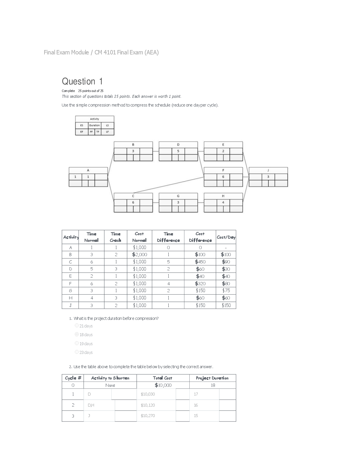
CEA 201 Final Exam | Verified with 100% Correct Answers There is a tremendous variety of products, from single-chip microcomputers costing a few dollars to supercomputers costing tens of millions of dollars that can ri
...
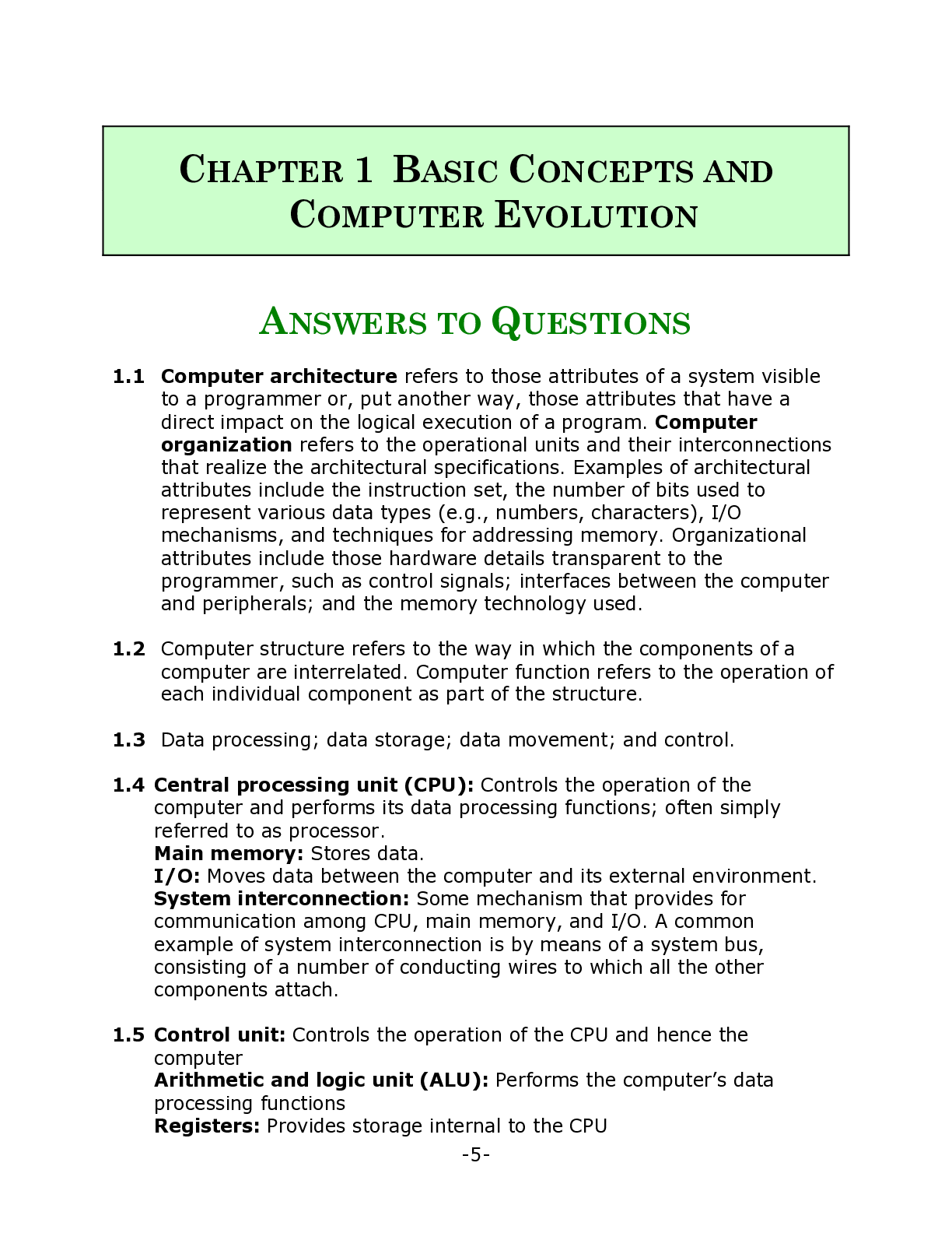
CEA 201 Final Exam | Verified with 100% Correct Answers There is a tremendous variety of products, from single-chip microcomputers costing a few dollars to supercomputers costing tens of millions of dollars that can rightly claim the name "computer". a. True b. False The variety of computer products is exhibited only in cost. a. True b. False Computer organization refers to attributes of a system visible to the programmer. a. True b. False Changes in computer technology are finally slowing down. a. True b. False The textbook for this course is about the structure and function of computers. a. True b. False The number of bits used to represent various data types is an example of an architectural attribute. a. True b. False Interfaces between the computer and peripherals is an example of an organizational attribute. a. True b. False Historically the distinction between architecture and organization has not been an important one. a. True b. False A particular architecture may span many years and encompass a number of different computer models, its organization changing with changing technology. a. True b. False A microcomputer architecture and organization relationship is not very close. a. True b. False Changes in technology not only influence organization but also result in the introduction of more powerful and more complex architectures. a. True b. False The hierarchical nature of complex systems is essential to both their design and their description. a. True b. False Both the structure and functioning of a computer are, in essence, simple. a. True b. False A computer must be able to process, store, move, and control data. a. True b. False When data are moved over longer distances, to or from a remote device, the process is known as data transport. a. True b. False Computer technology is changing at a __________ pace. a. slow b. slow to medium c. rapid d. non-existent Computer _________ refers to those attributes that have a direct impact on the logical execution of a program. a. organization b. specifics c. design d. architecture Architectural attributes include __________ . a. I/O mechanisms b. control signals c. interfaces d. memory technology used _________ attributes include hardware details transparent to the programmer. a. Interface b. Organizational c. Memory d. Architectural It is a(n) _________ design issue whether a computer will have a multiply instruction. a. architectural b. memory c. elementary d. organizational It is a(n) _________ issue whether the multiply instruction will be implemented by a special multiply unit or by a mechanism that makes repeated use of the add unit of the system. a. architectural b. memory c. mechanical d. organizational A __________ system is a set of interrelated subsystems. a. secondary b. hierarchical c. complex d. functional An I/O device is referred to as a __________. a. CPU b. control device c. peripheral d. register When data are moved over longer distances, to or from a remote device, the process is known as __________. a. data communications b. registering c. structuring d. data transport The _________ stores data. a. system bus b. I/O c. main memory d. control unit The __________ moves data between the computer and its external environment. a. data transport b. I/O c. register d. CPU interconnection A common example of system interconnection is by means of a __________. a. register b. system bus c. data transport d. control device A _________ is a mechanism that provides for communication among CPU, main memory, and I/O. a. system interconnection b. CPU interconnection c. peripheral d. processor _________ provide storage internal to the CPU. a. Control units b. ALUs c. Main memory d. Registers The __________ performs the computer's data processing functions. a. Register b. CPU interconnection c. ALU d. system bus The world's first general-purpose electronic digital computer was designed and constructed at The Ohio State University. a. True b. False John Mauchly and John Eckert designed the ENIAC. a. True b. False The major drawback of the EDVAC was that it had to be programmed manually by setting switches and plugging and unplugging cables. a. True b. False The IAS is the prototype of all subsequent general-purpose computers. a. True b. False The IAS operates by repetitively performing an instruction cycle. a. True b. False Backward compatible means that the programs written for the older machines can be executed on the new machine. a. True b. False A vacuum tube is a solid-state device made from silicon. a. True b. False Computers are classified into generations based on the fundamental hardware technology employed. a. True b. False System software was introduced in the third generation of computers. a. True b. False A wafer is made of silicon and is broken up into chips which consists of many gates and/or memory cells plus a number of input and output attachment points. a. True b. False IBM's System/360 was the industry's first planned family of computers. a. True b. False Intel's 4004 was the first chip to contain all of the components of a CPU on a single chip. a. True b. False Designers wrestle with the challenge of balancing processor performance with that of main memory and other computer components. a. True b. False The Intel x86 evolved from RISC design principles and is used in embedded systems. a. True b. False A common measure of performance for a processor is the rate at which instructions are executed, expressed as billions of instructions per seconds (BIPS). a. True b. False The _________ was the world's first general-purpose electronic digital computer. a. UNIVAC b. MARK IV c. ENIAC d. Hollerith's Counting Machine The Electronic Numerical Integrator and Computer project was a response to U.S. needs during _________. a. the Civil War b. the French-American War c. World War I d. World War II The ENIAC used __________. a. vacuum tubes b. integrated circuits c. IAS The ENIAC is an example of a _________ generation computer. a. first b. second c. third d. fourth The __________ interprets the instructions in memory and causes them to be executed. a. main memory b. control unit c. I/O d. arithmetic and logic unit The memory of the IAS consists of 1000 storage locations called __________. a. opcodes b. wafers c. VLSIs d. words The __________ contains the 8-bit opcode instruction being executed. a. memory buffer register b. instruction buffer register c. instruction register d. memory address register During the _________ the opcode of the next instruction is loaded into the IR and the address portion is loaded into the MAR. a. execute cycle b. fetch cycle c. instruction cycle d. clock cycle Second generation computers used __________. a. integrated circuits b. Transistors c. vacuum tubes d. large-scale integration The __________ defines the third generation of computers. a. integrated circuit b. vacuum tube c. transistor d. VLSI The use of multiple processors on the same chip is referred to as __________ and provides the potential to increase performance without increasing the clock rate. a. multicore b. GPU c. data channels d. MPC With the __________, Intel introduced the use of superscalar techniques that allow multiple instructions to execute in parallel. a. Core b. 8080 c. 80486 d. Pentium The __________ measures the ability of a computer to complete a single task. a. clock speed b. speed metric c. execute cycle d. cycle time ARM processors are designed to meet the needs of _________. a. embedded real-time systems b. application platforms c. secure applications d. all of the above One increment, or pulse, of the system clock is referred to as a _________. a. clock tick b. cycle time c. clock rate d. cycle speed The __________ are used to designate the source or destination of the data on the data bus. a. system lines b. data lines c. control lines d. address lines The von Neumann architecture is based on which concept? a. data and instructions are stored in a single read-write memory b. the contents of this memory are addressable by location c. execution occurs in a sequential fashion d. all of the above The TL supports which of the following address spaces? a. memory b. I/O c. message d. all of the above The interconnection structure must support which transfer? a. memory to processor b. processor to memory c. I/O to or from memory d. all of the above The data lines provide a path for moving data among system modules and are collectively called the _________. a. control bus b. address bus c. data bus d. system bus The unit of transfer at the link layer is a phit and the unit transfer at the physical layer is a flit. a. True b. False With asynchronous timing the occurrence of events on the bus is determined by a clock. a. True b. False It is not possible to connect I/O controllers directly onto the system bus. a. True b. False A key characteristic of a bus is that it is not a shared transmission medium. a. True b. False An I/O module cannot exchange data directly with the processor. a. True b. False Interrupts do not improve processing efficiency. a. True b. False A(n) _________ is generated by a failure such as power failure or memory parity error. a. I/O interrupt b. hardware failure interrupt c. timer interrupt d. program interrupt The processing required for a single instruction is called a(n) __________ cycle. a. execute b. fetch c. instruction d. packet Virtually all contemporary computer designs are based on concepts developed by __________ at the Institute for Advanced Studies, Princeton. a. John Maulchy b. John von Neumann c. Herman Hollerith d. John Eckert Each data path consists of a pair of wires (referred to as a __________) that transmits data one bit at a time. a. lane b. path c. line d. bus A(n) _________ is generated by some condition that occurs as a result of an instruction execution. a. timer interrupt b. I/O interrupt c. program interrupt d. hardware failure interrupt A __________ is the high-level set of rules for exchanging packets of data between devices. a. bus b. protocol c. packet d. QPI The QPI _________ layer is used to determine the course that a packet will traverse across the available system interconnects. a. link b. protocol c. routing d. physical A sequence of codes or instructions is called __________. a. software b. memory c. an interconnect d. a register A bus that connects major computer components (processor, memory, I/O) is called a __________. a. system bus b. address bus c. data bus d. control bus The _________ receives read and write requests from the software above the TL and creates request packets for transmission to a destination via the link layer. a. transaction layer b. root layer c. configuration layer d. transport layer The basic function of a computer is to execute programs. a. True b. False A key requirement for PCIe is high capacity to support the needs of higher data rate I/O devices such as Gigabit Ethernet. a. True b. False Because all devices on a synchronous bus are tied to a fixed clock rate, the system cannot take advantage of advances in device performance. a. True b. False Timing refers to the way in which events are coordinated on the bus. a. True b. False The method of using the same lines for multiple purposes is known as time multiplexing. a. True b. False In general, the more devices attached to the bus, the greater the bus length and hence the greater the propagation delay. a. True b. False Computer systems contain a number of different buses that provide pathways between components at various levels of the computer system hierarchy. a. True b. False Program execution consists of repeating the process of instruction fetch and instruction execution. a. True b. False At a top level, a computer consists of CPU, memory, and I/O components. a. True b. False No single technology is optimal in satisfying the memory requirements for a computer system. a. True b. False A typical computer system is equipped with a hierarchy of memory subsystems, some internal to the system and some external. a. True b. False External memory is often equated with main memory. a. True b. False The processor requires its own local memory. a. True b. False Cache is not a form of internal memory. a. True b. False The unit of transfer must equal a word or an addressable unit. a. True b. False Both sequential access and direct access involve a shared read-write mechanism. a. True b. False In a volatile memory, information decays naturally or is lost when electrical power is switched off. a. True b. False To achieve greatest performance the memory must be able to keep up with the processor. a. True b. False Secondary memory is used to store program and data files and is usually visible to the programmer only in terms of individual bytes or words. a. True b. False The L1 cache is slower than the L3 cache. a. True b. False With write back updates are made only in the cache. a. True b. False It has become possible to have a cache on the same chip as the processor. a. True b. False All of the Pentium processors include two on-chip L1 caches, one for data and one for instructions. a. True b. False Cache design for HPC is the same as that for other hardware platforms and applications. a. True b. False __________ refers to whether memory is internal or external to the computer. a. Location b. Access c. Hierarchy d. Tag Internal memory capacity is typically expressed in terms of _________. a. hertz b. nanos c. bytes d. LOR For internal memory, the __________ is equal to the number of electrical lines into and out of the memory module. a. access time b. unit of transfer c. capacity d. memory ratio "Memory is organized into records and access must be made in a specific linear sequence" is a description of __________. a. sequential access b. direct access c. random access d. associative Individual blocks or records have a unique address based on physical location with __________. a. associative b. physical access c. direct access d. sequential access For random-access memory, __________ is the time from the instant that an address is presented to the memory to the instant that data have been stored or made available for use. a. memory cycle time b. direct access c. transfer rate d. access time The ________ consists of the access time plus any additional time required before a second access can commence. a. latency b. memory cycle time c. direct access d. transfer rate A portion of main memory used as a buffer to hold data temporarily that is to be read out to disk is referred to as a _________. a. disk cache b. latency c. virtual address d. miss A line includes a _________ that identifies which particular block is currently being stored. a. cache b. hit c. tag d. locality __________ is the simplest mapping technique and maps each block of main memory into only one possible cache line. a. Direct mapping b. Associative mapping c. Set associative mapping d. None of the above When using the __________ technique all write operations made to main memory are made to the cache as well. a. write back b. LRU c. write through d. unified cache The key advantage of the __________ design is that it eliminates contention for the cache between the instruction fetch/decode unit and the execution unit. a. logical cache b. split cache c. unified cache d. physical cache The Pentium 4 _________ component executes micro-operations, fetching the required data from the L1 data cache and temporarily storing results in registers. a. fetch/decode unit b. out-of-order execution logic c. execution unit d. memory subsystem In reference to access time to a two-level memory, a _________ occurs if an accessed word is not found in the faster memory. a. miss b. hit c. line d. tag A logical cache stores data using __________. a. physical addresses b. virtual addresses c. random addresses d. none of the above The basic element of a semiconductor memory is the memory cell. a. True b. False A characteristic of ROM is that it is volatile. a. True b. False RAM must be provided with a constant power supply. a. True b. False The two traditional forms of RAM used in computers are DRAM and SRAM. a. True b. False A static RAM will hold its data as long as power is supplied to it. a. True b. False Nonvolatile means that power must be continuously supplied to the memory to preserve the bit values. a. True b. False The advantage of RAM is that the data or program is permanently in main memory and need never be loaded from a secondary storage device. a. True b. False Semiconductor memory comes in packaged chips. a. True b. False All DRAMs require a refresh operation. a. True b. False A number of chips can be grouped together to form a memory bank. a. True b. False An error-correcting code enhances the reliability of the memory at the cost of added complexity. a. True b. False DRAM is much costlier than SRAM. a. True b. False RDRAM is limited by the fact that it can only send data to the processor once per bus clock cycle.
[Show More]