University of Phoenix ECON 240 EarlHedgehog195
$ 9
eBook Pre-Calculus All-in-One For Dummies Book + Chapter Quizzes Online 1st Edition By Mary Jane Sterling
Electrical Engineering > QUESTIONS & ANSWERS > California Polytechnic State University, San Luis Obispo - EE 308EE308_HW6_F2012solutions (All)
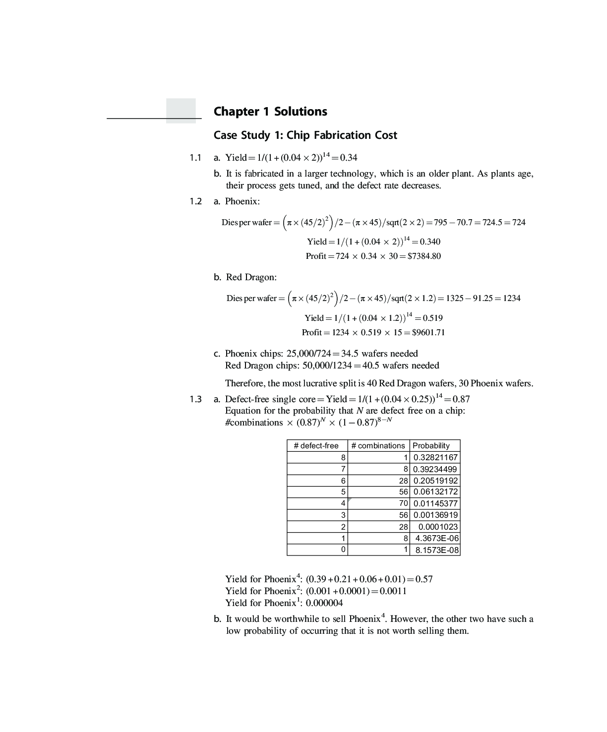
EE308 Analog Electronics and Integrated Circuits Assigned: 11/4/12 Due: 11/7/12 by 4:15pm (Turn in in class, slip under my door or turn in electronically. Electronic submissions due at 10pm) This ... assignment is more practice on amplifier design. It also asks a question or two on differential pairs. 1. Download the HW6DiffPair.asc file from PolyLearn and answer the following questions through simulations. All of the questions are about the region around the bias point. You will need to include the right model file. The model file is the same as for previous homeworks but you’ll need to fix the path. Assume differential input and differential outputs. a. Explain the biasing circuitry. ANSWER: You need the VBE for half the current of the tail current source for the load pnps of the diff pair. To do that, I put two pnp in parallel so half the current would go through each and then I used their VBE to bias the load pnps. b. What is the ADM for the circuit? ANSWER: Single-ended output is 3.233V with an input (single-ended) of 0.001V. Max Vout=7.31317V, min Vout=4.08483V. Max Vin=4.001V, min Vin=3.999V. ADM vod vid1 1 vid vod22 7.31317 3.999 V V4.08483 4.001V V 4 4. .001 08483 V V3.999 7.31317 V V 6.04566 .002 3228.3 c. What is the PSRR for the circuit from GND? Why? No simulation needed and no math needed. Assume you are in a legal small signal region. ANSWER: Since the output is differential, any noise that shows up on both outputs will be subtracted out. Assuming GND noise will be amplified the same on both sides, then PSRR will be infinite. d. What is the ACM for the circuit? ANSWER: Moving the inputs together I get: Max Vout=5.76928V, min Vout=5.63583V. Max Vin=4.1V, min Vin=3.9V. So: 0.66725 4.1 3.9 5.63583 5.76928 V V V V ACM Not great. If the loads would have been passive (resistors), then the ACM would have been about zero. e. What is the CMRR for the circuit? ANSWER: 4838.22 0.66725 3228.3 ACM ADM CMRR 2. Design an amplifier: a. Design an amplifier that, when the input is 5V, there is 20mA through it. Also, the Rin must be > 10KΩ and the Rout < 1.5Ω. The output must follow the input by some shift (not specified) but, between Vin=5.5V and Vin=4.5V, the change in the shift must be less than 1mV. The math must be shown for Rin and Rout but the variation in the shift can be shown through a simulation. Use VT=26mV and a Vsup of 8V. β=192.66. VA=100. VBEON=0.78V. Do math or else it will take you an extra long time to do this problem. Include calculations, final Rin, Rout and shift error values as well as a screen capture to show how you determined variation [Show More]
Last updated: 3 years ago
Preview 1 out of 5 pages

Buy this document to get the full access instantly
Instant Download Access after purchase
Buy NowInstant download
We Accept:

Can't find what you want? Try our AI powered Search
Connected school, study & course
About the document
Uploaded On
Apr 06, 2021
Number of pages
5
Written in
All
This document has been written for:
Uploaded
Apr 06, 2021
Downloads
0
Views
92
Scholarfriends.com Online Platform by Browsegrades Inc. 651N South Broad St, Middletown DE. United States.
We're available through e-mail, Twitter, Facebook, and live chat.
FAQ
Questions? Leave a message!
Copyright © Scholarfriends · High quality services·