Tcfp HazMat Operations Questions And Answers 2022( Latest Update) Download To Score An A.
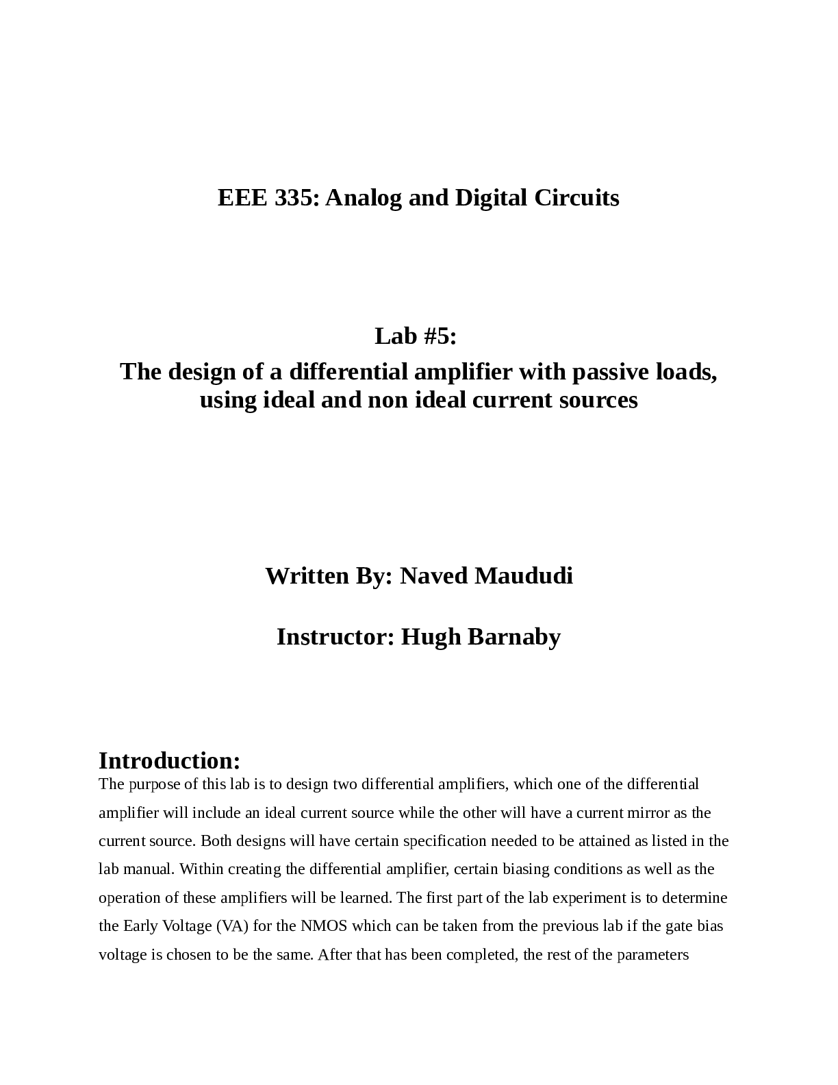
Electrical Engineering > Lab Report > Arizona State UniversityEEE 335Lab5report-Analog and Digital Circuits (All)
EEE 335: - Lab #5: The design of a differential amplifier with passive loads, using ideal and non ideal current sources Written By: Naved Maududi Instructor: Hugh Barnaby Introduction: The purp ... ose of this lab is to design two differential amplifiers, which one of the differential amplifier will include an ideal current source while the other will have a current mirror as the current source. Both designs will have certain specification needed to be attained as listed in the lab manual. Within creating the differential amplifier, certain biasing conditions as well as the operation of these amplifiers will be learned. The first part of the lab experiment is to determine the Early Voltage (VA) for the NMOS which can be taken from the previous lab if the gate bias voltage is chosen to be the same. After that has been completed, the rest of the parametersNMOS transistors are determined such as gate width, and voltage gate bias dependent on the gain specification as well as current limits. These are all DC bias points and are set based upon the conditions of the specification of the differential amplifier such as the voltage swing that the amplifier needs to exhibit as well as the current for current supply. It is important to note that both the NMOS transistors need to be in saturation at all times in order for the amplifier to operate correctly with the resistive load. Once the DC characterization and finalization of the parameters of the transistor have been chosen, the AC analysis begins. The small signal parameters for the circuit at hand are calculated by hand at first then compared to values attained from DC, transient, and AC stimulation. For this process, the differential gain, common mode gain, input resistance, and output resistance with respect to frequency are plotted. Also, within the design specification, the input amplitude is chosen so that the differential output exhibits at least a 2.5 V peak to peak. Also, within this section, the common mode rejection ratio is calculated as well as the total current in order to ensure that it does not exceed 0.5 milliamps. Objectives: There were many objectives in the lab which will be outlined below. The primary purpose of this lab is to design two differential amplifiers, one with an ideal current source and one with a nonideal current source such as a current mirror. Both of these amplifiers will have certain design specification as listed in the lab manual such as a total current supply less than 0.5 mA, the differential output voltage swing of about 2.5 volts peak to peak, and a differential gain of 10 V/V or above. These specifications need to be met for both the design of ideal and non-ideal differential amplifiers. The first part of the lab experiment is to determine the Early Voltage (VA) for NMOS transistor, which can be borrowed from the previous la [Show More]
Last updated: 3 years ago
Preview 1 out of 28 pages
Buy this document to get the full access instantly
Instant Download Access after purchase
Buy NowInstant download
We Accept:

Can't find what you want? Try our AI powered Search
Connected school, study & course
About the document
Uploaded On
May 01, 2021
Number of pages
28
Written in
All
This document has been written for:
Uploaded
May 01, 2021
Downloads
0
Views
87
Scholarfriends.com Online Platform by Browsegrades Inc. 651N South Broad St, Middletown DE. United States.
We're available through e-mail, Twitter, Facebook, and live chat.
FAQ
Questions? Leave a message!
Copyright © Scholarfriends · High quality services·


 (1).png)
.png)


.png)


.png)